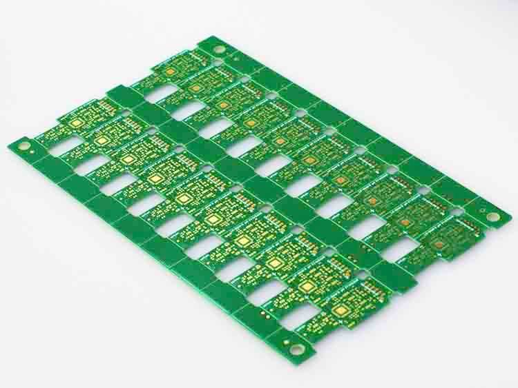
Printed Circuit Board
-
Standard Advanced Cutting Edge
-
Minimµm Inner Line Width 100 75 50
-
Minimµm Outer Space 100 100 75
-
Minimµm Outer Space 100 75 50
-
Minimµm Inner Space 100
Plotter Line
Manufacturing Capabilities
-
Number of layers: 1 – 52
-
Materials: High performance FR4, rigid polyimide, low loss hydrocarbon, low loss PTEF
-
Copper weights (finished): 18 μm – 105 μm
-
Minimum line/space: 0.075 mm / 0.075 mm
-
Minimum core thickness: 0.1 mm
-
Thickness range: 0.6 mm – 3.2 mm
-
Available panels dimensions: 610×457 or 560×457
-
Surface finishes available: HASL, LF HASL, OSP, ENIG
-
Minimum mechanical drill: 0.15 mm

-
Number of layers: 1 – 4 L
-
Materials: Flex polyimide
-
Copper weights (finished): 18 μm – 35μ
-
Minimum line/space: 0.075 mm / 0.075 mm
-
Minimum core thickness: 0.025 mm
-
Thickness range: 0.03 mm – 0.1 mm
-
Available panels dimensions: 610×457 or 560×457
-
Surface finishes available: OSP, ENIG
-
Minimum mechanical drill: 0.15 mm
-
Minimum laser drill: 0.075 mm

-
Number of layers: 4-16 layers
-
Materials: High performance FR4, Rigid polyimide, Flex Polyimide
-
Copper weights (finished): 18 μm – 70 μm
-
Minimum line/space: 0.075 mm / 0.075 mm
-
Minimum core thickness: For Flex (0.025 mm) For Rigid (0.1 mm
-
Thickness range: 0.4 mm – 3.2 mm
-
Available panels dimensions: 610×457 or 560×457
-
Surface finishes available: OSP, ENIG
-
Minimum mechanical drill: 0.15 mm
-
Minimum laser drill: 0.075 mm

-
Number of layers: 1 – 52
-
Materials: High performance FR4, rigid polyimide, low loss hydrocarbon, low loss PTEF
-
Copper weights (finished): 18 μm – 105 μm
-
Minimum line/space: 0.075 mm / 0.075 mm
-
Minimum core thickness: 0.1 mm
-
Thickness range: 0.6 mm – 3.2 mm
-
Available panels dimensions: 610×457 or 560×457
-
Surface finishes available: HASL, LF HASL, OSP, and ENIG
-
Minimum mechanical drill: 0.15 mm
-
Minimum laser drill: 0.05 mm
| Plated Through Hole | Minimum finished diameter 150 μm-Aspect Ratio for PTH: ≤ 15 |
| Blind Micro via | Minimum diameter 50μm (laser drilled) -Aspect Ratio for blind vias: ≤ 1 |
| µVias Treatment | Capped through vias and resin filled blind vias, Copper filled |
| Fine Line | Minimum track/spacing is 50 μm, ±10 tolerance |
| Layer Count | Standard up to 32, special requirement up to 50 after DFM evaluation |
| Flexible Layer Count | Up to 16 inner layers in a Rigid-Flex build up, special requirement after DFM evaluation |
| Sequential Lamination | Up to 3+N+3 (SBU), special requirement after DFM evaluation |
| Base Cu Thickness | Thin copper 9 μm, 12 μm, 18μm, 35 μm, 70 μmup to 105μm. |
| Minimum Inner Layer Thickness | 50 μm, special requirement after DFM evaluation |
| Minimum Prepreg Thickness | 50 μm(1 x PP106) or lower but after DFM evaluation (PP1027 or Pp1037) |
| Maximum PCB Thickness | !"#$%#&% '() ** special requirement up to 5.2 mm after DFM evaluation |
| Maximum PCB Dimensions | Multilayer: 420 x 525 mm, SS,DS 420X585 |
| Solder Mask | Spray Coating or screen printed (Green, Blue, Black, Red & White) |
| Solder Mask Capability | Solder Dam 75 μm standard and 50 μm special; Clearance down to 50 μm. |
| Vias Treatment | Tenting and plugging process like per IPC classification |
| Printing Application | Legend, Peelable mask. |
| Finishing | HASL with/without Lead; ENIG, OSP ; As per special requirements. |