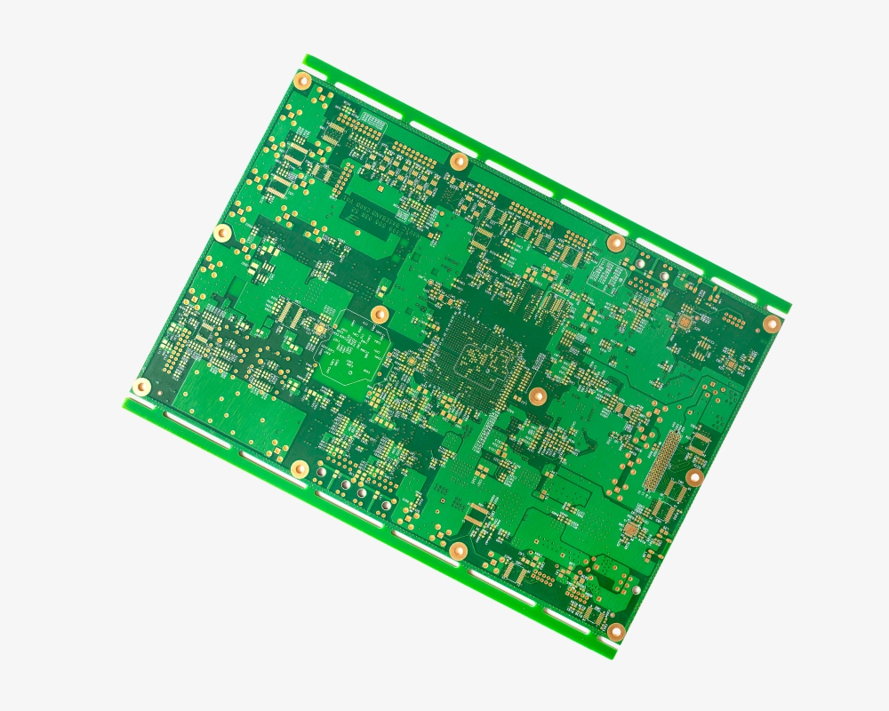
تصنيع الدوائر الألكترونية
تمتلك شركة الرواد للأنظمة خطوط إنتاج لتصنيع لوحات الدوائر المطبوعة أحادية الطبقة وثنائية الطبقة ومتعددة الطبقات حتى 52 طبقة بطاقة إنتاجية تصل إلى 10,000 متر مربع شهريًا، حيث نقوم بتصنيع دوائر إلكترونية صلبة ومرنة وعالية الكثافة باستخدام أحدث تقنيات التصنيع ووفقًا لأعلى معايير الجودة والسلامة.
Plotter
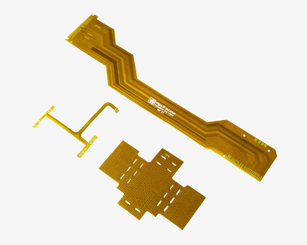
تصنيع الدوائر الألكترونية
تمتلك شركة الرواد للأنظمة خطوط إنتاج لتصنيع لوحات الدوائر المطبوعة أحادية الطبقة وثنائية الطبقة ومتعددة الطبقات حتى 52 طبقة بطاقة إنتاجية تصل إلى 10,000 متر مربع شهريًا، حيث نقوم بتصنيع دوائر إلكترونية صلبة ومرنة وعالية الكثافة باستخدام أحدث تقنيات التصنيع ووفقًا لأعلى معايير الجودة والسلامة.
Inner Layer Pretreatment
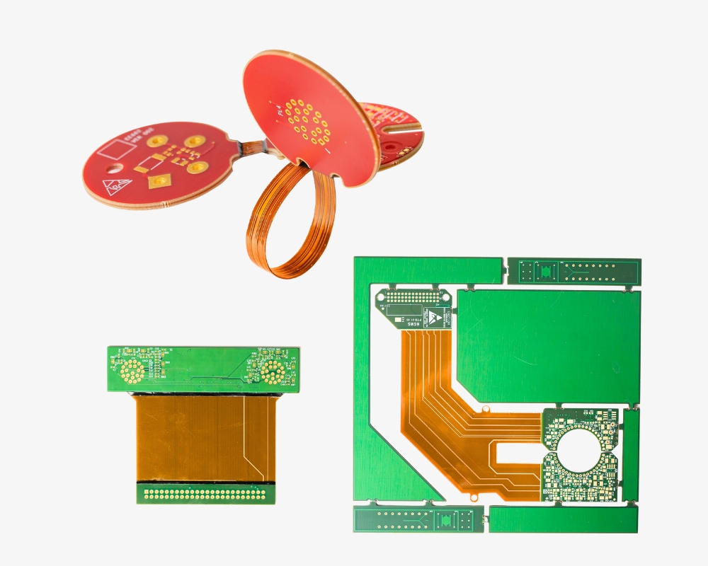
تصنيع الدوائر الألكترونية
تمتلك شركة الرواد للأنظمة خطوط إنتاج لتصنيع لوحات الدوائر المطبوعة أحادية الطبقة وثنائية الطبقة ومتعددة الطبقات حتى 52 طبقة بطاقة إنتاجية تصل إلى 10,000 متر مربع شهريًا، حيث نقوم بتصنيع دوائر إلكترونية صلبة ومرنة وعالية الكثافة باستخدام أحدث تقنيات التصنيع ووفقًا لأعلى معايير الجودة والسلامة.
Automated Optical Inspection
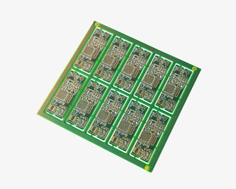
تصنيع الدوائر الألكترونية
تمتلك شركة الرواد للأنظمة خطوط إنتاج لتصنيع لوحات الدوائر المطبوعة أحادية الطبقة وثنائية الطبقة ومتعددة الطبقات حتى 52 طبقة بطاقة إنتاجية تصل إلى 10,000 متر مربع شهريًا، حيث نقوم بتصنيع دوائر إلكترونية صلبة ومرنة وعالية الكثافة باستخدام أحدث تقنيات التصنيع ووفقًا لأعلى معايير الجودة والسلامة.
Routing
تصنيع الدوائر الألكترونية
تمتلك شركة الرواد للأنظمة خطوط إنتاج لتصنيع لوحات الدوائر المطبوعة أحادية الطبقة وثنائية الطبقة ومتعددة الطبقات حتى 52 طبقة بطاقة إنتاجية تصل إلى 10,000 متر مربع شهريًا، حيث نقوم بتصنيع دوائر إلكترونية صلبة ومرنة وعالية الكثافة باستخدام أحدث تقنيات التصنيع ووفقًا لأعلى معايير الجودة والسلامة.
Final Inspection and Testing
قدرات التصنيع
-
عدد الطبقات: 1 – 52
-
المواد: FR4 عالي الأداء، بوليميد صلب، هيدروكربون منخفض الخسارة، PTEF منخفض الخسارة
-
أوزان النحاس (نهائية): 18 ميكرومتر – 105 ميكرومتر
-
الحد الأدنى للخط/المسافة: 0.075 مم / 0.075 مم
-
الحد الأدنى لسمك القلب: 0.1 مم
-
نطاق السماكة: 0.6 مم – 3.2 مم
-
أبعاد الألواح المتوفرة: 610×457 أو 560×457
-
التشطيبات السطحية المتاحة: HASL، LF HASL، OSP، ENIG
-
الحد الأدنى للمثقاب الميكانيكي: 0.15 مم
-
عدد الطبقات: 1 – 4 L
-
المواد: بولي أميد مرن
-
أوزان النحاس (نهائية): 18 ميكرومتر – 35 ميكرومتر
-
الحد الأدنى للخط/المسافة: 0.075 مم / 0.075 مم
-
الحد الأدنى لسمك القلب: 0.025 مم
-
نطاق السماكة: 0.03 مم – 0.1 مم
-
أبعاد الألواح المتوفرة: 610×457 أو 560×457
-
Surface finishes available: OSP, ENIG
-
الحد الأدنى للمثقاب الميكانيكي: 0.15 مم
-
الحد الأدنى لمثقاب الليزر: 0.075 مم
-
عدد الطبقات: 4-16 طبقة
-
المواد: FR4 عالي الأداء، بوليميد صلب، بوليميد مرن
-
أوزان النحاس (نهائية): 18 ميكرومتر – 70 ميكرومتر
-
الحد الأدنى للخط/المسافة: 0.075 مم / 0.075 مم
-
الحد الأدنى لسمك القلب: للمرن (0.025 مم) للصلب (0.1 مم)
-
نطاق السماكة: 0.4 مم – 3.2 مم
-
أبعاد الألواح المتوفرة: 610×457 أو 560×457
-
التشطيبات السطحية المتاحة: OSP، ENIG
-
الحد الأدنى للمثقاب الميكانيكي: 0.15 مم
-
الحد الأدنى لمثقاب الليزر: 0.075 مم
-
عدد الطبقات: 1 – 52
-
المواد: FR4 عالي الأداء، بوليميد صلب، هيدروكربون منخفض الخسارة، PTEF منخفض الخسارة
-
أوزان النحاس (نهائية): 18 ميكرومتر – 105 ميكرومتر
-
الحد الأدنى للخط/المسافة: 0.075 مم / 0.075 مم
-
الحد الأدنى لسمك القلب: 0.1 مم
-
نطاق السماكة: 0.6 مم – 3.2 مم
-
أبعاد الألواح المتوفرة: 610×457 أو 560×457
-
التشطيبات السطحية المتاحة: HASL و LF HASL و OSP و ENIG
-
الحد الأدنى للمثقاب الميكانيكي: 0.15 مم
-
الحد الأدنى لمثقاب الليزر: 0.05 مم
| Plated Through Hole | Minimum finished diameter 150 μm-Aspect Ratio for PTH: ≤ 15 |
| Blind Micro via | Minimum diameter 50μm (laser drilled) -Aspect Ratio for blind vias: ≤ 1 |
| µVias Treatment | Capped through vias and resin filled blind vias, Copper filled |
| Fine Line | Minimum track/spacing is 50 μm, ±10 tolerance |
| Layer Count | Standard up to 32, special requirement up to 50 after DFM evaluation |
| Flexible Layer Count | Up to 16 inner layers in a Rigid-Flex build up, special requirement after DFM evaluation |
| Sequential Lamination | Up to 3+N+3 (SBU), special requirement after DFM evaluation |
| Base Cu Thickness | Thin copper 9 μm, 12 μm, 18μm, 35 μm, 70 μmup to 105μm. |
| Minimum Inner Layer Thickness | 50 μm, special requirement after DFM evaluation |
| Minimum Prepreg Thickness | 50 μm(1 x PP106) or lower but after DFM evaluation (PP1027 or Pp1037) |
| Maximum PCB Thickness | Standard 3.2mm special requirement up to 5.2 mm after DFM evaluation |
| Maximum PCB Dimensions | Multilayer: 420 x 525 mm, SS,DS 420X585 |
| Solder Mask | Spray Coating or screen printed (Green, Blue, Black, Red & White) |
| Solder Mask Capability | Solder Dam 75 μm standard and 50 μm special; Clearance down to 50 μm. |
| Vias Treatment | Tenting and plugging process like per IPC classification |
| Printing Application | Legend, Peelable mask. |
| Finishing | HASL with/without Lead; ENIG, OSP ; As per special requirements. |
| ITEM | DESCRIPTION | STANDARD | ADVANCED | CUTTING EDGE |
| Track & Gap | Line / Space inner | 100 | 75 | 50 |
| Line / Space inner | 100 | 75 | 60 | |
| Minimum Outer Layer Annular Ring (OAR) on Production Hole Diameter (PHD | 150 | 100 | 75 | |
| Minimum Inner Layer Annular Ring (IAR) / Thermal Annular Ring on PHD | 150 | 100 | 75 | |
| Hole Diameter | Minimum Production Hole Diameter (PHD) for thickness 1.6 mm (Others: see table) | 200 | 150 | 150 |
| Maximum aspect ratio PTH: see also table (Thickness / PHD) | 8 | 12 | 15 | |
| μVia –Buried | Minimum blind μvia drill diameter -material with glass | 150 | 100 | 50 |
| Maximum blind μviaaspect ratio | 1 | 1 | 1.2 | |
| Minimum blind μvia drill diameter -material without glass | 125 | 100 | 50 | |
| μViatop pad annular ring | 150 | 100 | 75 | |
| μVialanding pad annular ring | 150 | 100 | 75 | |
| Maximum number of stack via | 1 | 2 | 3 | |
| Drill \Cu Distance | PTH to cu on inner layers (means IAR + Value) | 250 | 200 | 150 |
| NPTH to cu on inner layers /NPTH Routing always>250 μm(means IAR+Value) | 250 | 200 | 150 | |
| NPTH to cu on outer layers ( NPTH Routing always >200 μm) | 250 | 200 | 150 | |
| Routing Tolerance | 200 | 200 | 100 | |
| Solder Mask | Solder mask Registration +\-40 μm | +\-40 | +\-40 | +\-40 |
| Solder mask Thickness Above copper >=5 μm | >=5 | >=5 | >=5 | |
| Minimum SM DAM | 150 | 100 | 50 | |
| Build up | Maximum PCB thickness (mm) | 3.2 | 3.2 | 3.2 |
| Minimum PCB thickness tolerance (%) | 10 | 10 | 10 | |
| Maximum number of Layers for Rigid-Flex PCB | 8 | 12 | 16 |
| Material for Rigid PCB | Material for Flex PCB | High Frequency Materials |
| Isola 402, Isola 185Hr | DuPont PyraluxAP | Roger 3000 Series |
| Panasonic Megtron6 Isola P95 (Rigid Polyimid) | DuPont PyraluxLF | Roger 4000 Series |
| Any other material for special requirements. | Any other material for special requirements. | Any other material for special requirements. |